Research Stories
Plasma Processing Laboratory leading Next Generation Semiconductor Etching Technology
[ 2022 Distinguished Professor]
A novel atomic layer etching technology of two-dimensional semiconductors such as MoS2 has been developed first by this group and reported to Nature Communications.
Advanced Materials Science and Engineering
Prof.
YEOM, GEUNYOUNG
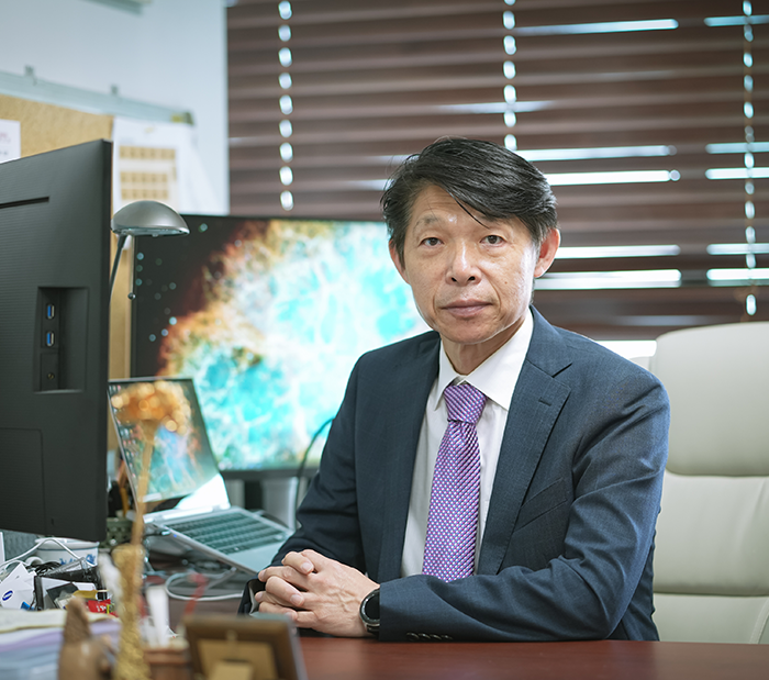
Professor Geun Young Yeom (Department of Advanced Materials Science&Engineering) has been selected as one of the distinguished professors of SKKU in 2022. His research group has been working on plasma etching technology for semiconductor devices which is one of the eight process technologies required for the fabrication of semiconductor devices. Here, plasma is an ionized gas known to be the 4th matter following sold, liquid, and gas, and it is used for various processing areas such as deposition, surface treatment, etching, etc.
To fabricate nanoscale semiconductors, first, extreme ultra-violet (EUV) light photolithographic technology forming a nano-size patterned polymer mask layer on the substrate is required. However, more importantly, a technology carving the underlying semiconductor layer along the nano-size mask layer formed by the photographic techniques is required and the technology carving the semiconductor material accurately as the mask layer shape is plasma etching technology.
Currently, the critical size of semiconductor devices is decreasing by less than a few nanometer scales and the semiconductor device structure is changing from a two-dimensional to a three-dimensional structure. Therefore, not only the etching techniques of various materials but also the deep/vertical etching methods for the formation of three-dimensional devices are required. Therefore, methods to etch nanometer scale materials vertically, selectively, without damaging the semiconductor materials, and accurately with atomic layer scale need to be investigated.
Prof. Yeom’s research group has been working on this state-of-the-art semiconductor etch technology for more than 30 years, and it is the most advanced research group on plasma etching technology in Korea actively working with Samsung Electronics, Samsung Display, SK hynix, and various semiconductor equipment companies to lead semiconductor etching technology in the world. Recently, a novel atomic layer etching technology of two-dimensional semiconductors such as MoS2, which are widely investigated as the next generation semiconductor materials replacing silicon material, has been developed first by this group and reported to Nature Communications. Also, the textbook “Plasma Etching Technology” written in 2006 by Prof. Yeom is known to be the “must read” engineering book for plasma etch engineers working on semiconductor device fabrication. Therefore, Prof. Yeom received a Minister Award from the Ministry of Commerce in 2016 for his contribution to the display industry and also received Presidential Award in 2016 for his contribution to the semiconductor industry.
Prof. Yeom was not only selected as a distinguished professor in 2002 from SKKU but also selected as a Fellow in 2022 by the American Vacuum Society (AVS), an American Scientific Research Society, that organizes conferences related to semiconductor equipment and processes. He also will receive a Nishizawa Award in Nov. 2022 from the Dry Process Symposium (DPS), a Japanese Scientific Research Society, specializing in semiconductor materials, equipment, and processes.